Machines have personalities. At least that's how it seems to a lot of engineers working on machine startups. Two machines with exactly the same bill of materials can have unique operating quirks that only a master engineer can tame.
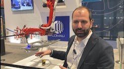
This is often the case with tool subsystems such as semiconductor wafer-handlers, and in particular wafer-handling robots for cleanroom wafer processing stations (Figure 1).
If only a fab technician--someone skilled at maintaining material flow and performing general maintenance, but not an expert robot teacher--could install, setup, and restart a robot at the touch of a single button.
If a robot builder could find and embed a system like that, the value-add to its customers would provide a significant market advantage. Asys (www.asys-llc.com), a German builder of wafer-handling robots for semiconductor tool systems installed in North America, Europe, and Asia, believes it has found both the solution and the advantages that come with it.
Handle With Care
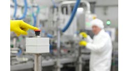
Wafer-handling robots move valuable and fragile semiconductor wafers to and from the process modules that make up semiconductor fabrication tools (Figure 2). They are taught the positions of extremely precise wafer pickup and delivery points. Such teaching may need to be done several times a year for each tool. Sometimes it is required unexpectedly when a tool "is not behaving."
This often leads to increased reliance on arbitrary diagnostic and troubleshooting skills and an inevitable increase in machine downtime. It also leads to unhappy customers. Avoiding these troublesome issues was high on the list for Asys. The company found the answer in the selection of a controller with an autocalibration capability.
"It takes an experienced technician hours to successfully teach a typical semiconductor tool," says Heinrich Walk, director of marketing for Asys. "Teaching is a difficult task. Close attention is required to avoid damaging the tool. Inaccurate teaching can result in tool production stoppages and even broken semiconductor wafers."
Robot teaching takes place in the pristine clean rooms of multibillion-dollar semiconductor fabs. Dressed in clean room garb and leaning into an out-of-service tool worth perhaps a million dollars, the teacher subjectively eyeballs a series of wafer handoff points to within about plus or minus a quarter millimeter.
Clearly, a big problem with this method of manual teaching is subjectivity. Some technicians are very good at teaching a tool and some are not. There can be substantial variations in taught points from one teaching episode to the next. Teaching subjectivity greatly impacts tool reliability. Poor teaching risks damage to wafers that may be worth tens of thousands of dollars apiece.
"It often takes eight hours," says Walk. "It depends on the technician. Some can do it in five hours and some take 16 hours. Contrast that to typically less than 20 minutes required for automated teaching in a tool equipped with autocalibration technology. That's a huge reduction in tool downtime."
It was therefore imperative for Asys to thoroughly investigate the available technology and determine the appropriate autocalibration tool for its systems. The search led to Berkeley Process Controls.
Finger on the Button
Asys found Berkeley carried a good reputation in the semiconductor industry. "Their controller's multitasking, shared-state information and capable user-programmable software layer gave us confidence that we could successfully implement important robot control capabilities," says Walk. "Capabilities such as collision avoidance, intelligent error recovery, autocalibration, robot self-diagnostics, and predictive maintenance fulfill key needs."
In tools equipped with Berkeley Autocalibration, an Asys technician simply presses a button to initiate automated robot teaching--rather than spending hours bent over inside a tool. "A preprogrammed routine precisely finds critical tool physical reference features and related wafer handoff positions in just minutes," says Walk. "As human factors are eliminated, teaching is accurate and highly repeatable."
The controller is programmed to drive an Asys robot motor to move its arm to a commanded position and to process I/O data. High-resolution encoders provide feedback to the controller indicating the present position of each motor. The controller software continuously compares the actual motor feedback position and the software-commanded motor position to generate appropriate drive signals. The controller's integrated drives provide necessary drive motor current.
"Touch calibration is the most powerful Autocalibration feature," says Nate Harding, Berkeley's mechanical engineering manager. "No added hardware or sensors are required."
The controller has real-time knowledge of the present velocity and torque of each robot motor and the present position of the robot's end effector. "The controller also knows the approximate location of the wafer handoff positions and the geometry of the end effector based upon previous information provided by the tool application developer," adds Harding.
When some users first hear about touch calibration, they picture robots being intentionally crashed into something. "That's because they've seen tool-damaging crashes due to robot control inadequacies," adds David Taylor, Berkeley's director of engineering.
"One OEM has even developed a 'foam block test.' The robot they're evaluating is run into a reference foam block at a specified speed and the deflection of the foam block is measured. They have a maximum deflection specification. The 'touch' of our touch calibration is very gentle,-as required when you're dealing with sensitive semiconductor manufacturing tools."
With touch calibration, the controller commands the Asys robot to slowly move the end effector into the predefined nominal location of a wafer handoff position. When the end effector makes light contact, that axis slows further and the motor torque changes, indicating physical contact. The controller instantly captures the encoder position as the calibration point.
Since the controller is aware in real time of the precise torque requirements of each motor, touch calibration is achieved with very low contact forces. Sophisticated torque data processing algorithms eliminate false triggers and ensure calibration consistency despite robot mechanism aging and changing friction characteristics.
No Options Required
Autocalibration technology implemented via a robot's laser wafer-mapping device also has the appeal of requiring no additional hardware or sensors. "Such mappers are normally used to accurately detect the edges of wafers in a wafer carrier or FOUP (front opening unified pod)," says Walk. "In this type of autocalibration implementation, the robot moves the laser mapper a small distance up and down while moving it slowly toward the nominal reference location. Upon the mapper's reflective optical detection of the reference edge, the controller instantly captures encoder position data as the calibration point."
Autocalibration technology can be implemented in a similar manner by adding through-beam or reflective optical sensors physically associated with wafer handoff positions.
"Autocalibration technology has been implemented with a wide variety of robot vendors' mechanical designs," says Taylor. "The controller architecture enables an effective implementation of the technology with both legacy belt-drive robot designs and state-of-the-art direct drive robots."
In addition to having typically greater positioning accuracy and repeatability, newer direct-drive robots have greater torque sensitivity, which enables superb touch calibration sensitivity.
Although autocalibration technology provides an automated teaching process, its value can only be recognized if it can demonstrate repeatable recognition of devices. "In a laboratory test, we recorded positions calculated by our Autocalibration technology for a wafer transfer station using a modern direct-drive robot," says Harding. "The data shows repeatability of better than +/-0.2 mm."
In a different semiconductor application, Berkeley reports autocalibration technology eliminates the need for precision mechanical alignment of shelves in a 12-FOUP (wafer cassette) storage buffer. The buffer employs a fast two-axis gantry equipped with a FOUP gripper. The autocalibration routine uses optical emitter-detectors and torque sensitivity to rapidly reference features on each storage shelf and on a master FOUP, thereby precisely and repeatably calibrating the system in minutes.
Sidebar:
Sequence of Events
A typical autocalibration sequence in a simple semiconductor front end proceeds as follows:
1. Laser wafer mapper calibration to height reference (Z position) of the master FOUP (a calibration fixture) on each pod door opener (PDO).
2. Touch calibration to reference post on master FOUP (X, Y position) on each PDO.
3. Laser wafer mapper calibration to top (Z position) of chuck on pre-aligner.
4. Touch calibration to pre-aligner chuck (X, Y position).
5. Calibration to pre-aligner optical sensor using the sensor (X, Y position).
6. Application-specific (sensor, mapper, and/or touch) calibration to wafer process handoff location (X, Y, Z position).
Sidebar:
Collision Insurance Required
"Ferraris on a wafer." That's how one major microprocessor manufacturer describes these slices of silicon. The company estimates the mid-range value for one of today's 300 mm wafers at $80,000-100,000 per wafer in eventual end product. Lower volume, leading-edge devices go well beyond this, while low-end devices are about $10,000.
For 200 mm wafers--fabs are still making high and low-end devices on them--$35,000-45,000 each is a reasonable estimate.
Getting a sense of wafer handling failures (caused by the robots) is a closely held statistic among fabricators. Some anecdotal information indicates chemical-mechanical polishing (CMP) machines range from approximately 1,000 hours MTBF at the lower end to 3,000 hours, which seems consistent with wet bench tool performances claimed at 1,500-2,000 hours MTBF. Since process failures in these machines are pretty unusual--the wafers sit in chemical tanks or in slurries--the problem areas are in the wafer handling, so the numbers should correlate closely to wafer handling reliability.
Robots by themselves often are touted at 50,000-plus hours MTBF. This is an indication that complexity, risk, and failures are due to the integration of the wafer handling operations.