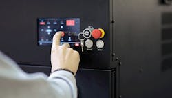
Interfaces have advanced significantly. The very idea of a wireless personal mobile device being used as a human-machine interface (HMI) was pie in the sky 10 years ago. An operator would, at the very least, need a hardened, industrialized tablet to survive the harsh environments and the constant dropping of the device.
And yet, here we are, not only using phones on the plant floor, but taking the interface home and interfacing remotely.
Also read: HMI software often starts with the hardware
Just when you thought it was safe to go back in the factory, UCLA researchers have designed ultrathin films suitable for application on human body contours that could lead to on-skin sensors and can turn biomechanical activities, such as the pressure of a finger tap, into electrical signals.
Xiangfeng Duan, professor of chemistry and biochemistry, and Yu Huang, professor and chair of the Materials Science and Engineering Department at the UCLA Samueli School of Engineering, co-leaders of the research team, compare the membrane’s stretchability to that of kitchen cling wrap with semiconducting electronic functionality.
The van der Waals thin film (VDWTF) is held together by intermolecular interactions, known as van der Waals forces, that can only take place at extremely close distances between atoms or molecules. And it could open myriad applications, such as sensing and signaling. Plus, it can be powered by the wearer’s movements, making it sustainable.
The 10-nanometer-thick membrane could connect HMIs, robotics and artificial-intelligence-enabled technologies.
The layered patchwork composition of the membrane comprises several even thinner layers, and, instead of being held in place by rigid covalent bonds, the layers are loosely connected by the nonbonding van der Waals forces. This allows the sheets to slide and rotate over one another.
Duan and Huang are both members of the California NanoSystems Institute (CNSI) at UCLA. The research was supported by the UCLA Physical Sciences Entrepreneurship and Innovation Fund, with additional support from the CNSI Noble Family Innovation Fund. The authors also acknowledge technical support from Electron Imaging Center at UCLA and the Nanoelectronics Research Facility at UCLA.
The UCLA Technology Development Group has applied for a patent on the technology. And applications are already being tested.

Mike Bacidore is the editor in chief for Control Design magazine. He is an award-winning columnist, earning a Gold Regional Award and a Silver National Award from the American Society of Business Publication Editors. Email him at [email protected].
About the Author

Mike Bacidore
Editor in Chief
Mike Bacidore is chief editor of Control Design and has been an integral part of the Endeavor Business Media editorial team since 2007. Previously, he was editorial director at Hughes Communications and a portfolio manager of the human resources and labor law areas at Wolters Kluwer. Bacidore holds a BA from the University of Illinois and an MBA from Lake Forest Graduate School of Management. He is an award-winning columnist, earning multiple regional and national awards from the American Society of Business Publication Editors. He may be reached at [email protected]